
Intel took us on a particular go to to its superior chip packaging, meeting, and testing services positioned on the island of Penang, and one other one within the mainland metropolis of Kulim, Malaysia and it was fairly an expertise.
Through the tour, we visited two services. The Penang Meeting and Check (PGAT) facility is the place the silicon dies are assembled, validated, and examined for errors. Then, the Intel Kulim Die Kind Die Prep (KMDSDP) facility is the place the actual magic occurs. This facility processes silicon wafers and readies these silicon wafers for die preparation and categorization for packaging and testing at Intel services worldwide.
We have got the silicon, however now, what after that
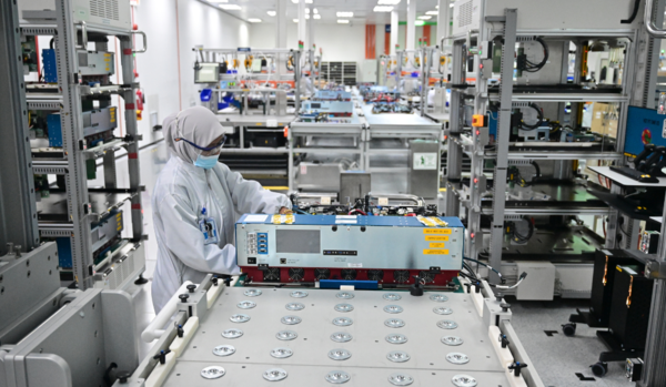
Kulim Die Kind Die Prep (KMDSDP) facility has two most important operations – die preparation and sorting. These days, 300mm wafers are the usual measurement produced, and they’re acquired at Kulim. Right here, they endure a collection of processes that singulate them into particular person chips.
Wafers are hooked up to versatile mylar sheets and undergo numerous processes, comparable to grinding and thinning to a precise profile, to create particular person chips. Utilizing a vacuum and UV gentle, chips are separated and positioned into trays earlier than sorting. Intel makes use of large sorting modules, as massive as a bus, with 20 take a look at cells weighing 1,000 kilos every, to check and kind the chips. It was so yellow in there that it felt like we had been within the Mexico.
A specifically designed lifting mechanism that hovers above the ground utilizing a cushion of air manoeuvres these modules. Chips are loaded onto trays and distributed to varied take a look at cells.
One of many assessments is to make sure that the chips are dependable and free from defects; each undergoes testing utilizing a probe card. The probe card consists of hundreds of skinny needles which might be even thinner than human hair, which connect with the built-in circuit contained in the take a look at gear. This enables for the measurement of the chip circuits’ electrical energy and evaluation of any defects that could be current.
Then, there are computerized guided automobiles to move these trays all through the testing facility.
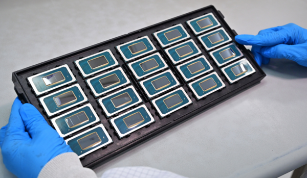
After a tray goes by the testing and characterization section, it’s returned to the realm the place the wafer was lower into particular person chips. The chips that don’t cross the take a look at are separated, thrown away, or recycled. The trays with chips which have efficiently handed all of the assessments are sorted and assigned a selected SKU. Every chip is faraway from the tray and sealed between two movie layers. The sealed chips are then rolled onto a reel to be transported to the Meeting and Check services positioned worldwide for additional processing.
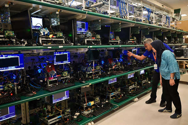
Intel additionally makes its personal testing gear
Through the go to to Intel’s facility, we additionally visited the System Integration and Manufacturing Companies (SIMS) facility, which manufactures testing gear for CPUs.Among the machines which might be manufactured on this facility embrace the excessive–density Burn-In (HDBI) tester, the Excessive-Density Modular Tester (HDMT) tester, and the System Stage Tester (SLT). These gear are utilized by Intel services in Malaysia and worldwide to check the CPUs.
A sneak peek into Intel’s testing practices
One of many Meeting and Check services is in Penang, the place these chips are acquired and endure additional processing and testing earlier than it reaches OEMs. Upon receiving the reels, the ability removes the die, and packages and conducts testing earlier than the chips are distributed. PGAT’s meeting and take a look at course of has six levels.
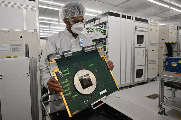
The primary is Chip Connect, the place the chip is bonded to the substrate utilizing the Foveros face-to-face (F2F) chip-on-chip bonding course of. An additional layer of epoxy underfill is added to take away microscopic gaps. The subsequent step is to connect the Built-in Warmth Spreader (IHS) utilizing thermal interface materials and adhesive. This enables for environment friendly warmth dissipation. Now, the CPU is prepared, however there may be one final step earlier than it may be despatched out to OEMs.
On the Design And Growth Lab in Penang, the CPU undergoes burn-in, electrical, and PPV testing. The chips are uncovered to excessive temperatures and voltages to determine defects. As soon as handed, all electrical traces and functionalities are examined. Then, these undergo PPV testing, which is to verify performance in precise buyer pc methods by simulating assessments in managed environments. Now, these CPUs are lastly able to be loaded up within the vehicles and attain their vacation spot.